News Center
A new type of electronic materials company that is based on independent research and development, integrating development, production, sales, and service.
Omdia: 28nm will become a long-node process technology for semiconductor applications in the next 5 years.
Release time:
2020-12-04
Current wafer foundry status of 28nm
Guided by Moore's Law, the line width of integrated circuits continues to shrink, basically progressing at a pace of reducing to 70% of the original size every two years. For example, it reached 45nm in 2007, 32nm in 2009, and 22nm in 2011. The 28nm process is between 32nm and 22nm, and the industry introduced the second generation of high-k dielectric/metal gate process at 32nm based on the earlier 45nm (HKMG) process, laying the foundation for the gradual maturity of 28nm. 2013 was the year of popularization for the 28nm process, and between 2015 and 2016, the 28nm process began to be widely used in mobile application processors and basebands. The limit of planar design on wafers can achieve optimized costs at 28nm. In contrast, the subsequent 16/14nm processes require the introduction of FinFET technology, which will increase wafer manufacturing costs by at least 50%, and only applications with a large volume, such as mobile, can share the costs. In many non-consumer-related applications, the stability of the 28nm process, as well as its performance and cost parameters, are very cost-effective.
With the maturity of 28nm process technology, the market demand for 28nm process products has shown explosive growth, and this high growth trend continued until 2017. From 2015 to 2016, the main application areas of the 28nm process were still mobile processors and basebands. After 2017, although the application of the 28nm process in the mobile field has declined, its application in several other fields has rapidly increased, such as OTT boxes and smart TVs, where the market growth rate is relatively fast. The capacity distribution is shown in the figure below, and the huge production reserves are also to prepare for the development of more emerging application fields in the future.
Figure 1: Advanced technology capacity, 28 nanometer and below (includes 32-nanometer)
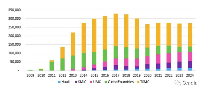
Source: Omdia
Main chip products in China at 28nm and new chip products that may be introduced in the next 5 years
From the revenue trend of pure wafer foundry, excluding the high profits of advanced processes led by TSMC, other foundries' revenues mainly come from stable and mature processes. Among pure wafer foundry companies, UMC, Globalfoundries, SMIC, etc., have all steadily improved performance and introduced various new products on 28nm (and related derivative processes) to meet different customer needs.
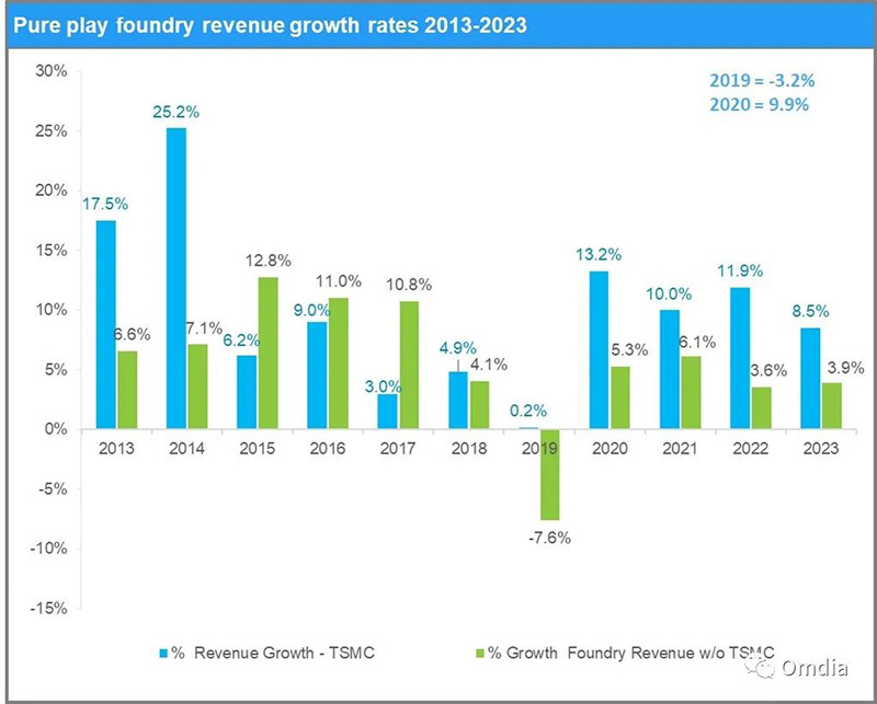
Source: Omdia
According to Omdia's observations, the following products will become mainstream on the 28nm production line, and considering comprehensive cost and performance, they will remain stable in production at 28nm for a relatively long period.
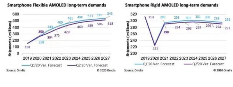
OLED Driver
With the improvement of mobile configurations and the continuous release of OLED panel capacity, the growth of OLED will bring an increase in demand for OLED Drivers. Currently, OLED Drivers are mainly concentrated in Korean manufacturers, and 28nm is about to become the mainstream process for high-end OLED Drivers (low power consumption, smaller SRAM area) in the next 3-5 years.
Figure 3: Smartphone OLED long-term demands
Connectivity Chips
The explosion of IoT applications and the upgrade of traditional household appliances have increased the demand for wireless connections such as WIFI and Bluetooth on various application terminals. Currently, mainstream wireless connection technologies have migrated to 28nm technology. Future upgrades in industrial and consumer sectors will inevitably drive a large demand for wireless connections.
FPGA
FPGAs have huge application space in various proprietary application fields, such as composite computing centers, wireless base stations, and autonomous vehicles. The 28nm process is a relatively optimized choice in terms of computing performance and overall power consumption.
Navigator (GNSS, Beidou, GPS)
With the successful networking of China's Beidou navigation, applications with Beidou navigation functions will become increasingly common. Currently, navigation chips, especially those with Beidou capabilities, all start from the 28nm design process, and the future application space is vast.
4G Transceiver
Although 5G mobile phones have entered a rapid growth phase, there is still huge growth potential for 4G mobile phone sales, and the mainstream design process for 4G transceivers is 28nm.
Edge Computing
The combination of cloud and edge computing has led to an increasing demand for local computing on the edge. Currently, edge computing generally has simple artificial intelligence analysis capabilities, and 28nm is very advantageous for applications that require localized data collection and preliminary logical computing capabilities.
NB-IoT, LoRA, Cat.1, eMTC
SoC chips with mainstream IoT protocols are mainly designed with 28nm and will become a long-term mainstream choice.
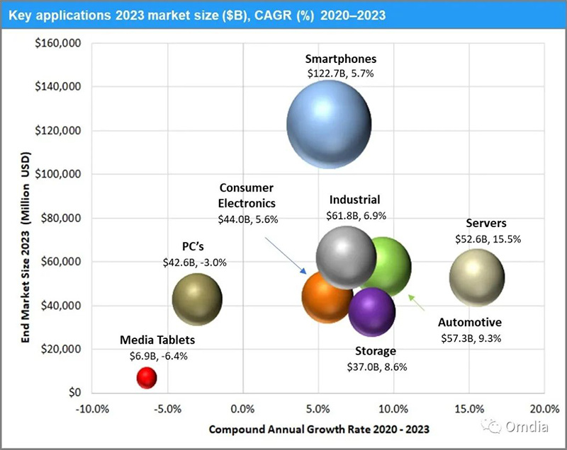
Emerging application fields and market development trends in the next five years
In recent years, with the upgrade of new hardware on mobile devices and the rise and popularization of the Internet of Things, the emergence of more and more new applications has led to the 28nm process entering the next period of strong demand.
Source: Omdia
Conclusion
Although 28nm is a very good high-cost-performance process, competition among foundries at this node is becoming increasingly fierce. In addition to TSMC, UMC, Samsung, Globalfoundries, and SMIC, Huahong has also joined the fray.
Due to the development of Moore's Law reaching the 28nm process node, a different situation has emerged. Starting from 28nm, the development towards higher nodes, such as 20, 16, 14, 10, and 7nm, means that the cost of each transistor in integrated circuits no longer decreases but increases.
Of course, in the face of the challenges of FinFET, Samsung and Globalfoundries have successively introduced FD-SOI technology. For SOI processes, the 28nm process has more advantages and can last a long time. Moreover, as the process advances, SOI will become increasingly advantageous. 28nm is considered a dividing point. At this node, the process can easily transition to SOI.
We will see that due to the commercialization of 5G, we are about to achieve a fully digital connected world. Chips, as the foundational point, will be increasingly adopted in various technological upgrades and innovations. The evolution of advanced processes driven by mobile devices and the ubiquitous computing and connectivity demanded by the Internet of Everything will become the dual driving forces of future semiconductors. Undoubtedly, 28nm will provide a stable and solid foundational supply for building the Internet of Everything.
Focus on hot spots


Contact Us
009 Chaoyang Road, Shitan Industrial Park, Quanjiao County, Chuzhou City, Anhui Province

Sweep
WeChat official account