News Center
A new type of electronic materials company that is based on independent research and development, integrating development, production, sales, and service.
IEDM: New interconnection technology beyond 3nm
Release time:
2020-02-17
During a short course on a Sunday at the last IEDM, Chris Wilson from imec presented new interconnect technologies suitable for nodes below 3nm.
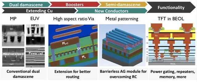
Advancing nodes requires DTCO and scaling boosters, such as self-aligned blocks (SAB), fully self-aligned vias (FSAV), supervias, and buried power rails (BPR). Chris reviewed the essence of the processes for most of the aforementioned scaling boosters, but I will not repeat all the details here, as I am not a process expert.
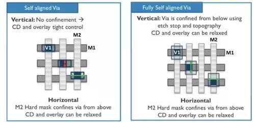
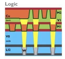
But here is an example of a fully self-aligned via (FSAV). Fully self-aligned means that the via is constrained by both the interconnect layer below and the interconnect layer above, as shown in the figure below, so the metal material of the via is exactly in the position needed to connect the two interconnect layers.
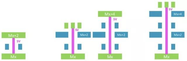
Supervia is another technology that is very meaningful for design. The first generation of supervia can connect from Mx to Mx+2 (whereas the usual via connects from Mx to Mx+1), which is very useful in SRAM. The second generation of supervia can connect from Mx to Mx+3 or Mx+4, suitable for buried power rails. Then the third generation supervia connects directly from Mx to Mx+5, allowing it to jump directly to lower resistance interconnect layers.
Buried power rails allow standard cells using single fin devices or nanosheet devices to scale from 6-track to 5-track, thus reducing cell area by 17% without scaling the pitch. Since the power rails are now located at the bottom of the entire stack, supervias help connect the power lines to higher interconnect levels, allowing power to be supplied to the cells on the chip, as shown in the figure.
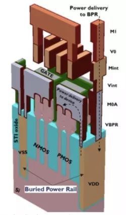
Using ruthenium as a conductive material and a high aspect ratio BPR can achieve an electrical performance of 50Ω/μm.
Extension of copper process
A major issue with copper is that it requires a barrier layer/pad layer; otherwise, copper will migrate into the surrounding oxides. However, it is difficult to scale the barrier layer and pad layer as finely as the scaled interconnect lines themselves, which means that as the interconnect lines scale, the proportion of copper becomes smaller. Moreover, on the path where current flows from the upper via to the lower interconnect line, each via also has such an unscalable barrier layer/pad layer at its bottom. When interconnect scaling reaches a half-pitch of 16nm and below, we need a barrier layer/pad layer with a thickness of less than 2nm. Perhaps we can use ruthenium to make a barrier layer/pad layer of 2nm thickness, but at a thickness of 1nm, we currently have no alternative materials.
Hybrid metallization schemes (cobalt, the yellow part in the image, without a barrier layer) make copper filling easier, and there is no barrier layer at the bottom of the via.
Beyond copper process
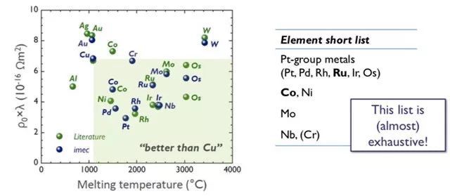
This chart shows all the metals that are "better than copper" because they have higher melting points and lower resistivity. We want higher melting points because they are beneficial for electromigration.

Here are just a few attractive metal material options. Attractive metals are cobalt (Co) and ruthenium (Ru). For barrier-free Ru with the same trench cross-section, its performance at a line width of 16nm is better than Cu. For barrier-free Co, its performance is better than Cu at a line width of less than 12nm.
A major challenge of the cobalt process is the CMP process, as metal electrochemical corrosion occurs in the trenches, so a different alkaline cleaning process needs to be replaced after cleaning. The CMP process is also a challenge for the ruthenium process, and its extensive use depends on the final choice of feature sizes. The adhesion strength of ruthenium to oxides also poses challenges. However, imec has manufactured 21nm pitch ruthenium metal lines that have passed the TDDB (Time-Dependent Dielectric Breakdown) and electromigration tests with a lifespan indicator of 10 years.
Another approach is to abandon the dual damascene copper process in favor of metal etching (the interconnect technology before the copper process). This is beneficial for resistivity and is also applicable to ruthenium. Additionally, due to less grain boundary scattering, this process has a resistivity advantage. This can allow the metal pitch to reach a critical size of 14nm, and annealing can also adjust the resistivity.
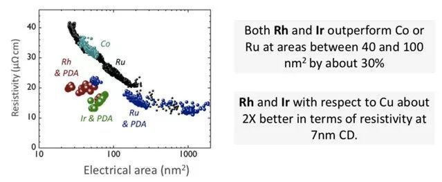
The line resistivity of rhodium (Rh) and iridium (Ir) is better than that of ruthenium and cobalt. There are also some complex compounds that exhibit excellent performance and may be used to address the issue of increasing resistance.
Summary
Chris's summary:
BEOL requires scaling boosters and DTCO to enhance process capabilities for device architecture.
Pre-filling (using Co or Ru) can provide a stepping stone for alternative metals.
However, interconnects will require alternative metals such as Co or Ru.
The damascene process of ruthenium metal is feasible at a pitch of 21nm and has passed all reliability indicators, but faces scaling challenges at a pitch of 16nm.
The metal etching process of ruthenium can provide a 20-30% RC advantage for interconnects below a pitch of 16nm.
There is a range of materials that can help combat the rise in resistance.
Focus on hot spots


Contact Us
009 Chaoyang Road, Shitan Industrial Park, Quanjiao County, Chuzhou City, Anhui Province

Sweep
WeChat official account