News Center
A new type of electronic materials company that is based on independent research and development, integrating development, production, sales, and service.
Transistor selection after 1nm: CFET?
Release time:
2020-09-16
At VLSI 2020, IMEC published an interesting paper on monolithic CFET, and I had the opportunity to interview one of the authors, Airoura Hiroaki. It is well known in the industry that FinFET (FF) is approaching its scaling limits. Samsung has announced that they will switch to Horizontal Nanosheets (HNS) at 3nm. TSMC will maintain 3nm FF but is expected to transition to a new architecture at 2nm.
Assuming Intel was still pursuing its own technology at that time, it is expected that Intel will retain 7nm FF before migrating to 5nm HNS.
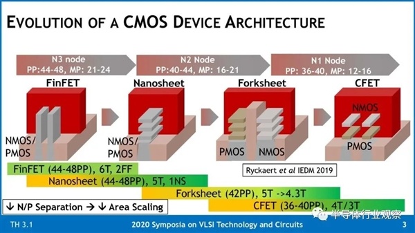
The most likely roadmap for the industry is to transition from FF to HNS with or without Forksheets, and then to CFET (Complementary FETs), see Figure 1.
Imec CMOS roadmap.
From the above technology blueprint, 28nm used High-K/Metal Gate, 16nm---14nm introduced FinFET, 7nm---5nm adopted EUV lithography equipment, and Co was also applied to Middle of Line (MOL).
MOL is a via that connects transistors (FOEL) with multi-layer wiring (BEOL). Although imec used Co, there are other options such as Mo, Ru, etc.
In addition, transistors with Nanosheet structure were used in 4nm---3nm.
At this VLSI symposium, there were many articles published regarding 7nm, 5nm, and 3nm; however, the author found that the application of Gate All Around (GAA) Nanosheet structure at these nodes is a globally common understanding.
At the same time, from the technology blueprint perspective, at 2nm, Forksheet transistors equipped with Buried Power Rail (BPR, a structure where power lines are buried under the transistor) will be used; at 1nm, Complementary FET (CFET) using BPR will be employed.
imec reached the following consensus internally: Nanosheet for 3nm, Forksheet for 2nm, CFET for 1nm.
In other words, at this VLSI symposium, imec also made statements based on the above technology blueprint. It is clear from the above figure how the structures of FinFET, Nanosheet, Forksheet, and CFET have changed.
From FinFET to CFET, by minimizing Contact Poly Pitch (PP) and separating nMOS and pMOS, the effect of reducing SRAM area is achieved.
Forksheet and CFET reduce size by stacking nFET and pFET devices to improve the spacing from n to p, see Figure 2.
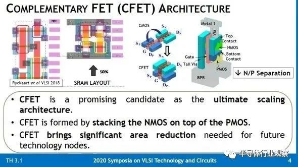
The CFET structure has developed a 'monolithic' CFET in current work, which involves using separate wafers for nFET and pFET and then bonding them together, while in the sequential method, CFET will manufacture both types of FET on the same wafer.
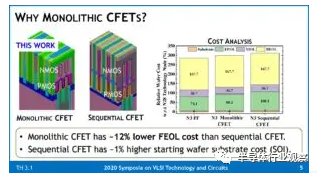
Imec claims that monolithic technology is cheaper than sequential technology, while sequential technology requires SOI, which increases substrate costs by 1%, see Figure 3.
The cost advantage of monolithic CFET at 1nm is that IMEC adopts CFET with nMOS and pMOS arranged vertically (as shown in Figure 8). Although the CFET process flow is very complex, it undoubtedly greatly reduces the area of CMOS and SRAM, achieving integration. The question is whether the characteristics of the transistors that people expect have been achieved, which is key to future research and development.
I found that the starting wafer cost is about 1% higher for two reasons: first, I do not believe that sequential CFET requires SOI, and second, SOI is about 1% more expensive than standard wafers. The overall approach will also require two starting wafers, not just one.
I believe this cost analysis needs more investigation. In the monolithic approach, nFET and pFET are manufactured on separate wafers, allowing for optimization of the manufacturing process for each device. The processing flow for each wafer is shown in Figure 4.
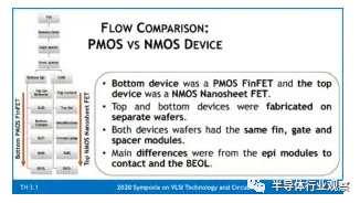
Figure 4. Process flow of monolithic CFET.
As we move towards N3, the separation from n to p reduces parasitic effects and improves performance. Similarly, by moving from FF to GAA, a gate can be provided on all four sides instead of three, improving electrostatic control.
The monolithic CFET manufactured in this work provides an alternative to sequential CFET for next-generation devices, requiring further research.
Focus on hot spots


Contact Us
009 Chaoyang Road, Shitan Industrial Park, Quanjiao County, Chuzhou City, Anhui Province

Sweep
WeChat official account